Difference between revisions of "Muonpi board"
| Line 25: | Line 25: | ||
=== Digital Pulse Processor === | === Digital Pulse Processor === | ||
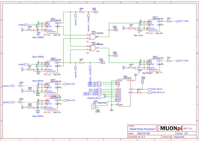
| + | [[File:Digital-pulse processor v3.1.png|thumb|640px|Digital pulse processor (V3.1)]] | ||
=== GNSS Module === | === GNSS Module === | ||
Revision as of 11:02, 23 November 2020
The MuonPi board is designed as plug-on board for the Raspberry Pi B+ in a form factor conforming with the RPi HAT specifications.
Contents
Functional Description
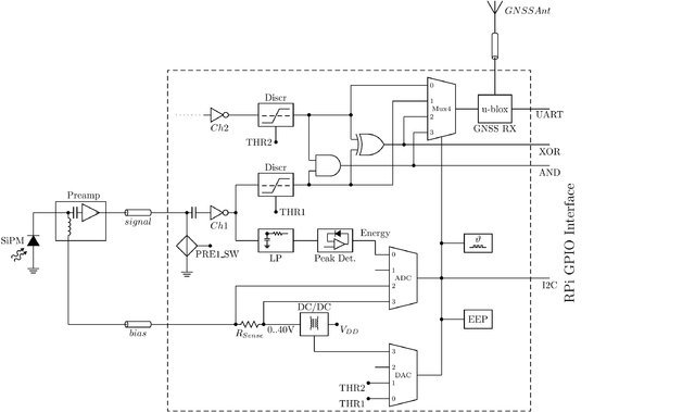
The MuonPi board implements following functionalities:
- Two input channels
- Supply voltage for remote powering the preamplifier through the signal line: The voltage can be switched on/off through a GPIO signal (individually for the two channels). It includes overcurrent and overtemperature shutdown and a fault signal.
- Bias voltage supply for the SiPM sensor and bias voltage/current supervision. A DC/DC converter generates the required reverse biasing voltage from the RPi 5V rail. The voltage can be switched on/off through a GPIO signal. Actual bias voltage and current are measured through the on-board ADC. The voltage can be controlled through the on-board DAC (not in HW version 2).
- Optional inverter for the two signal inputs (mounting option) in case negative signals are presented to the board
- Threshold discriminators with adjustable thresholds (DAC channels 1 and 2) in the range from 0.5 mV to 3V. The discriminator outputs are LVCMOS signals with a length of ~100 ns.
- Both channels are logically connected by one AND gate and one XOR gate. In this way, a coincidence ("both at the same time") as well as an anti-coincidence ("only exactly one") within a 100 ns time window can be asserted.
- The two gate signals (AND/XOR) are time-shaped to 1 us length and provided to the GPIO interface of the RPi
- The two discriminator signals and the two logic gate signals are fed to a multiplexer. Its output is fed to the time stamping input of the u-blox GNSS receiver.
- The u-blox GNSS receiver NEO-M8N is utilized to get the precise time and frequency reference in order to provide a sufficient precision of the time stamping on the nanosecond level. The time stamp of an event (leading and trailing edges of the signal present at the multiplexer output) is transmitted to the RPi via UART interface through the UBX-TIM-TM2 message.
Detailed Description
The MuonPi board design is open hardware. It is entirely defined in the free EDA cloud tool EasyEDA. The current working version of the design is HW Ver 2 which is explained in detail below. For the predecessor version (HW Ver 1) follow this link. The recent development version (HW Ver 3) is currently in testing.
Input Stage
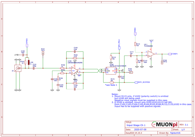
The signal input comprises a 50 Ohms-terminated signal path with simultaneous provision of the bias voltage (VPRE1) for remote powering of the preamplifier. The AC component is decoupled and provided to a differential wide-band amplifier LMH6550 with a voltage gain of ~3. In this way, the output is symmetrical around a mid-scale common mode voltage yielding a non-inverted and an inverted signal. An analog switch SN74LVC1G3157 selects either one depending on the switch control input (POL1) and presents the capacitively coupled signal to a fast comparator TLV3502. The threshold THR1 is provided from the DAC (see "RPi Interface").


