Difference between revisions of "Silicon photomultiplier"
Tag: Undo |
|||
| (5 intermediate revisions by the same user not shown) | |||
| Line 6: | Line 6: | ||
== Principle of Photodiodes == | == Principle of Photodiodes == | ||
A SiPM detector is formed by a pixelated matrix of photodiodes. Each photodiode consists of a junction of positively and negatively doped silicon ('''p-n junction'''). A depleted region which is devoid of free charge carriers is formed in between the differently doped silicon materials. By applying a reverse-voltage to the photodiodes, the depleted region can be enlarged to extend through the entire sensor. | A SiPM detector is formed by a pixelated matrix of photodiodes. Each photodiode consists of a junction of positively and negatively doped silicon ('''p-n junction'''). A depleted region which is devoid of free charge carriers is formed in between the differently doped silicon materials. By applying a reverse-voltage to the photodiodes, the depleted region can be enlarged to extend through the entire sensor. | ||
| + | The passage of ionizing radiation through a photodiode creates electron-hole pairs. These liberated charge carriers are accelerated by the electric field in the depleted region towards the anode (holes) or cathode (electrons). | ||
| − | The | + | == The Geiger Mode == |
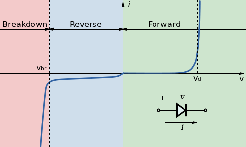
| + | [[File:Iv characteristic diode.png|frame|right|Current-Voltage characteristic of a diode. A SiPM operates in the Breakdown regime.]] | ||
| + | |||
| + | If the reverse-voltage is high enough to exceed the breakdown voltage of the p-n junction, the diode is said to operate in '''Geiger-mode'''. The energy of a single charge carrier accelerated by the electric field is sufficient to create additional electron-hole pairs which in turn liberate even more charge carriers. Ultimately, the multiplication process can lead to a self-sustaining avalanche. | ||
| + | == SiPM Photosensors == | ||
| + | |||
| + | When combining a multitude of photodiodes designed and operated as described in the previous sections, a SiPM detector is formed. The size of individual pixels (or diodes) ranges from 10 to 100 micrometres. | ||
Latest revision as of 17:59, 4 April 2020
Silicon photomultipliers (abbrev. SiPM) are photon-sensitive detectors operating as Single-photon avalanche diodes (SPAD).
Principle of Photodiodes
A SiPM detector is formed by a pixelated matrix of photodiodes. Each photodiode consists of a junction of positively and negatively doped silicon (p-n junction). A depleted region which is devoid of free charge carriers is formed in between the differently doped silicon materials. By applying a reverse-voltage to the photodiodes, the depleted region can be enlarged to extend through the entire sensor. The passage of ionizing radiation through a photodiode creates electron-hole pairs. These liberated charge carriers are accelerated by the electric field in the depleted region towards the anode (holes) or cathode (electrons).
The Geiger Mode
If the reverse-voltage is high enough to exceed the breakdown voltage of the p-n junction, the diode is said to operate in Geiger-mode. The energy of a single charge carrier accelerated by the electric field is sufficient to create additional electron-hole pairs which in turn liberate even more charge carriers. Ultimately, the multiplication process can lead to a self-sustaining avalanche.
SiPM Photosensors
When combining a multitude of photodiodes designed and operated as described in the previous sections, a SiPM detector is formed. The size of individual pixels (or diodes) ranges from 10 to 100 micrometres.
