Muonpi board
The MuonPi board is designed as plug-on board for the Raspberry Pi B+ in a form factor conforming with the RPi HAT specifications.
Contents
Functional Description
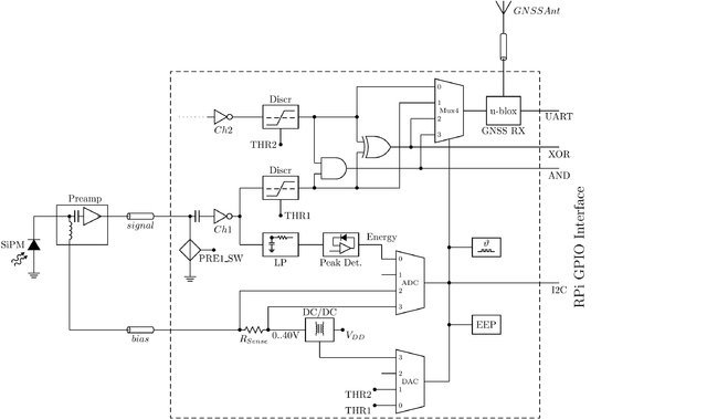
The MuonPi board implements following functionalities:
- Two input channels
- Supply voltage for remote powering the preamplifier through the signal line: The voltage can be switched on/off through a GPIO signal (individually for the two channels). It includes overcurrent and overtemperature shutdown and a fault feedback signal.
- Bias voltage supply for the SiPM sensor and bias voltage/current supervision. A DC/DC converter generates the required reverse biasing voltage from the RPi's 5V rail. The voltage can be switched on/off through a GPIO signal. Actual bias voltage and current are measured through the on-board ADC. The voltage can be controlled through the on-board DAC (not in HW version 2).
- Signal inverters for the two signal inputs in case negative signals are presented to the board
- Threshold discriminators with adjustable thresholds (DAC channels 1 and 2) in the range from 0.5 mV to 3V. The discriminator outputs are LVCMOS signals with a length of ~100 ns.
- Both channels are logically connected by one AND gate and one XOR gate. In this way, a coincidence ("both at the same time") as well as an anti-coincidence ("only exactly one") within a 100 ns time window can be asserted.
- The two gate signals (AND/XOR) are time-shaped to 1 us length and provided to the GPIO interface of the RPi
- The two discriminator signals and the two logic gate signals are fed to a multiplexer. Its output is fed to the time stamping input of the u-blox GNSS receiver.
- The u-blox GNSS receiver NEO-M8N is utilized to get the precise time and frequency reference in order to provide a sufficient precision of the time stamping on the nanosecond level. The time stamp of an event (leading and trailing edges of the signal present at the multiplexer output) is transmitted to the RPi via UART interface through the UBX-TIM-TM2 message.
Detailed Description
The MuonPi board design is open hardware. It is entirely defined in the free EDA cloud tool EasyEDA. The current working version of the design is HW Ver 3 which is explained in detail below.
The predecessor versions are available for reference: HW Ver 2 and HW Ver 1.
Input Stage
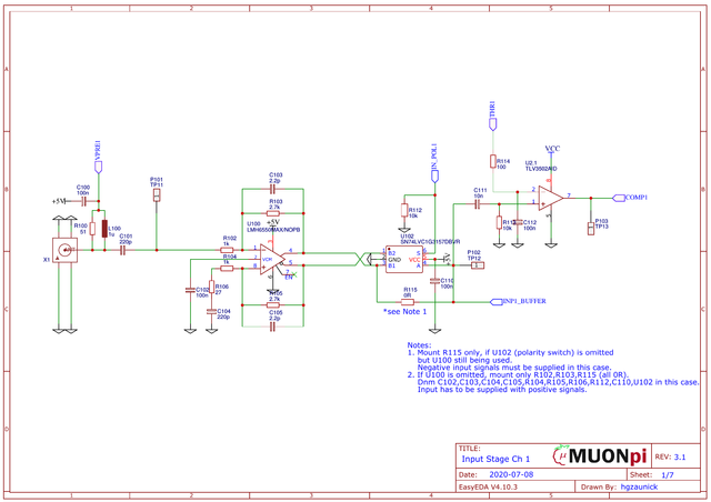
The signal input comprises a 50 Ohms-terminated signal path with simultaneous provision of the bias voltage (VPRE1) for remote powering of the preamplifier. The AC component is decoupled and provided to the differential wide-band amplifier U100/U200 (LMH6550) with a voltage gain of ~3. In this way, the output is symmetrical around a mid-scale common mode voltage with a non-inverted and an inverted signal superimposed. The analog switch U102/U202 (SN74LVC1G3157) selects either one depending on the switch control input (POL1) and presents the capacitively coupled signal to a fast comparator U2 (TLV3502). The threshold THR1 is provided from the DAC U402 (see "RPi Interface").
Digital Pulse Processor
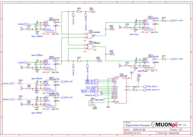
The outputs of comparator U2 are time-shaped with monostable gate U300 to 100 ns wide pulses. These are indicated as discriminator outputs for both channels. They are logically connected with both, AND gate U304 (which is actually a NOR gate but with the inverted inputs acting as an AND) as well as XOR gate U303. These signals are shaped to 1 us pulse length and supplied to GPIO pins (EVT_XOR and EVT_AND). The discriminator signals are also time-shaped to ca. 100 ms length by U306 to drive the indicator LEDs for a discernible visual signal. With the multiplexer U305 (74AC151), one of the signals (EVT_AND, EVT_XOR, DISCR1, DISCR2, TIMEPULSE) connected to its inputs can be selected and fed to the output TIME_MEAS. The selection word is supplied by the I2C-expander U404 (PCF9536). The selected output is routed to the interrupt pin of the u-Blox NEO GNSS chip where the rising edge is timestamped with nanosecond resolution and sent as UBX message TIM-TM2 over the UART interface to the host. The discriminator signals, time-shaped logic gates and the inverted multiplexer output are all series terminated in order to avoid false triggering or wrong timing due to reflections whereas the non-inverted multiplexer output driving only the u-Blox interrupt pin is terminated with a Thevenin matching network at the end (see GNSS receiver).
GNSS Receiver
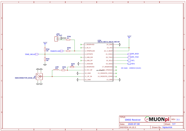
The u-Blox NEO M7/M8N receiver chip U700 processes the timing information from the GNSS satellites (GPS, Galileo, Glonass, BeiDou, QZSS, SBAS) and synchronizes its local TCXO to this time grid. The GNSS antenna is connected to SMA jack X7. The u-Blox chip provides a supply voltage for the antenna's preamplifier through R700/L700. The digital pulses are fed into the interrupt pin EXTINT0 for timestamping of both, rising and falling edges. The line is terminated by the Thevenin matching network R702/R703 which is driven by the output of multiplexer U305 with sufficient current. Note, that only the AC-family type has sufficient drive strength. Don't replace with other logic families. Communication with the chip is done via UART interface connecting directly to the RPi's TxD/RxD serial lines. Additionaly, the I2C interface is connected to the board's I2C bus. As it turned out, the communication via I2C requires a master capable of clock stretching. This feature is currently not available on the RPi hardware I2C interface, so the u-Blox I2C interface is currently not used. The 1pps time pulse is, additional to its distribution to a GPIO pin and the indicator LED409, routed to a the 2-pin pinheader connector J700 (TP_OUT) where it is available for other purposes. The u-Blox pps output can be programmed to other frequencies which may be utilized e.g. for PLL synchronization or disciplining a local oscillator (GPSDO).
RPi Interface
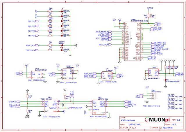
The interface of the MuonPi HAT connects to the 40-pin GPIO header of the Raspberry-Pi with several digital I/Os, the UART interface from the u-Blox chip and the interface to the on-board I2C bus. The four-channel ADC U401 (ADS1015/1115) acquires the voltages of the (optional) peak detector for the pulse amplitude measurement (ch1), the on-board supply voltage (nominal 3.3V, shifted into the ADC's input range by voltage divider R418/R419) on ch2 and the sense voltages (after the voltage dividers R505/506 and R507/508) at both ends of the sense resistor R504 (see "Power section") connected to channels 3 and 4, respectively. The 12-bit DAC U402 (MCP4728) provides a fine-grained adjustment of the two threshold voltages (THR1, THR2 on channels 1 and 2) and the control voltage on channel 3 for the DC/DC converter around U502. Channel 4 is not used, but routed to a through-hole pad "DAC4" where it may be used for any purpose. There are two I2C EEPROM chips on the board. U400 (24AA02UID) is for the MuonPi's specific storage of calibration parameters and the factory-programmed unique ID, while U405 (CAT24C32WI) which is actually connected to the RPi ID-I2C interface foreseen for exacly this purpose, provides the configuration parameters for HAT identification and automatic GPIO and boot overlay selection during the boot phase. Furthermore, the temperature sensor U403 (LM75A/B) and the 4-bit I/O expander U404 (U404) are also controlled via the on-board I2C bus. The I/O expander chip U404 provides the selection bit pattern for the multiplexer U305.
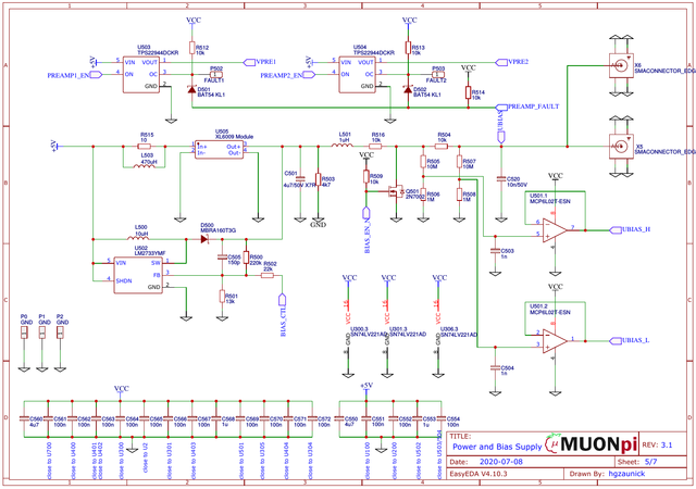
Power/Bias Supply
The bias voltage generation for the SiPM photo detector is foreseen in two ways, each one selected depending on the mounting. By default, the bias voltage of <33V is generated by the DC/DC converter around U502 (LM2733Y). It's output voltage is controlled by the voltage provided by channel 3 of the DAC (U402) with an intercept point set by the resistive divider network R500 to R502. The filtered output is shunted to ground by R503 to avoid a varying load of the converter circuit. After RF-filtering by L501, the voltage is passed through the current limiting series resistor R516 and shunted by n-mosfet Q501 which short-cuts the voltage to ground, when the BIAS_EN_N control signal is low. Otherwise, the non-zero output voltage is passed through the current measurement shunt R504. The symmetrical resistive dividers R505/R506 and R507/R508 tap the voltages at either side of R504 which are low-pass filtered through C503/C504 and buffered by U501 before routed to ADC channels 3 and 4. This circuit realizes both, measurement of the actual bias voltage as supplied to the SiPM as well as the measurement of the bias current.
