Montageanleitung
This is a guide on how to populate our MuonPi-PCB, using the construction kit. You can get a kit or a fully assembled PCB by contacting us here.
All components in this kit (except for the pin headers) are surface-mount devices (SMD). Most of these parts are only a few millimeters in size and are prone jump very far, should you slip with the tweezers. Soldering these requires steady hands and a bit of technique, but this guide aims to help you with that.
Contents
The Kit
The Kit contains all the parts you need to set up your very own particle detector using your Raspberry Pi.
Contents of the Kit are:
- The plastic scintillator (generously provided by Eljen Technology)
- The bare printed circuit board (Muonpi board)
- GNSS antenna
- Components to mount on the PCB (Resistors, Capacitors, Inductors, ICs, etc.)
- Bill of materials (BOM). There's also an interactive online version which simplifies the search for components on the board and has a place-and-tick checkmark for the already mounted components to maintain the overview during soldering.
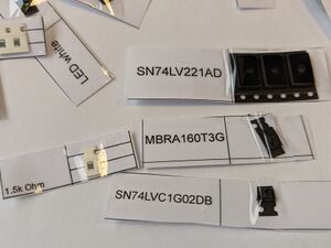
The individual components of the kit are glued to a nametag using tape, as can be seen in the picture.
Because of the size and difficulty labeling the parts, they are packaged using paper labels and clear tape. Getting the parts out of their packaging has to be done quite carefully, as they are easy to lose.
Tools
The bare essential tools are:
- soldering iron
- solder
- (metal) tweezers
- solder fume extractor
additional:
- flux
- solder wick
- vise or helping hands
- scalpel/scissors
- magnifying glass
Additionally, we recommend to choose a brightl workplace, as dim lights and small components can lead to eye strain and head aches.
Generally,the smaller the tip of your soldering iron is, the better, for small component soldering at least.
Of course if you have other solder tips, like ones with a solder depot, you can use those too.
In any case whatever tools you need to get the job done, are the correct tools to use.
Documentation
The schematic, layout and BOM of the current hardware version can be found on the easyEDA project page. While soldering, finding the right pad, where a specific components has to go, can be quite difficult. The labels on the PCB are small and space for them is very limited which makes some of them hard to read and find. To help you find the correct solder pads, we recommend to have a computer nearby where you can open the schematics and use the search function. Alternatively you can print out the layout that is attached on the easyEDA project page.
Mounting Options
The BOM specifies multiple mounting options, such as: "Full", "Single Channel", "External Bias Supply", "Fixed Input Polarity". "External Bias Supply" and "Fixed Input Polarity" were used by us in the development and will not be discussed here further. The default configuration of the kit contains only one scintillator, therefore only one channel of the detector electronics will be used at a time. In that case, the "Single Channel" mounting option would be sufficient. However the number of components in the kit follows the "Full" configuration, and mounting all components is still recommended. Just mounting all the parts that are included in the kit will lead to a working PCB with both channels working. Please contact us, if you are interested in a two scintillator setup.
Assembly
First things first, you should setup your workspace with all parts layed out, along with the BOM and all the tools you might need. Personally, I like to sort the parts into categories: Resistors, Capacitors, Inductors, ICs and others. This helps to save time and gives a quick overview of your soldering progress. In principle the choice which components to mount first comes down to personal preference. A helpful guideline is to mount parts depending on their height. Lower, smaller parts should be mounted first, as to not interfere too much in the later stages of assembly. This is why the GPIO headers should be among the last components to be mounted.
Once you are set up, you can turn on your soldering iron and fume extractor and start soldering.
Tips on SMD soldering
SMD components are small and difficult to solder.
The easiest components to solder are the resistors and capacitors.
Start with these to get comfortable with SMD soldering first, then proceed to the more difficult ICs.
A quick guide to SMD soldering can be found at sparkfun.com.
Be careful with the tip of the iron and the PCB. Too much heat and scraping of the pads can remove the top layer from the PCB or even rip the pad off the PCB. The later, depending on the pad this happens to, is very likely to completely brick the board and rendering it unusable.
Soldering Workflow
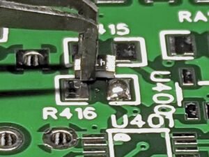
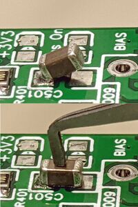
Take your BOM and choose one of the resistor/capacitor values to begin with and identify the pad label, where the part is supposed to be placed. Now take your soldering iron and heat one side of the pad. After a couple of seconds of heating, add some solder to the pad. Take out one of the components out of it's packaging and grab onto it with the tweezers as indicated in the picture on the right. Heat the solder blob and slide the component into the molten solder from the side. This ensures covering of the components contacts. Placing the component into the blob from above can lead to solder bridges underneath the component, which will render the component useless.
Once one side of the component is fixed, it's good practice to lightly press down on the component and remelt the solder. Doing this will help to mount the component flush to the board. Although not always necessary, doing this will help to avoid solder bridges, especially between the legs of ICs.
It is a good idea to cross out the components on the BOM once they are soldered. Should in the end a label on the BOM be left unmarked you can check to not miss any components.
When you are finished soldering all parts of one kind, pause and check you haven't missed any. Only then move on to the next group of parts.
Integrated Circuits (ICs)
Once all passive Components are placed and double checked, we can move on to the integrated circuits. Soldering these is considerably more difficult, especially the ADC and DAC (U401 & U402 in v3.x) have a very small pad pitch. Solder bridges are almost unavoidable and need to be dealt with.
First, solder is added to one pad on a corner of the IC footprint. Then, just like the passive components, the IC is moved into the molten solder. It is very important to align all the legs of the IC on their respective pads. Proceed to fix one of the other legs, preferably a leg on the diagonally opposite side. The remaining unsoldered legs can now be soldered to the board.
If solder bridges are created, they need to be removed. One possible method to remove solder bridges is the usage of flux. Flux is a mixture of multiple compounds that remove and prevent build up of oxides on the solder blob. Additionally it increases the surface tension of the molten solder and therefor promotes splitting of solder blobs. So just using a good amount of flux can fix solder bridges.
However if there is too much solder on the pads, bridges cannot be fixed just using flux. In that case we need to remove some solder. Solder wicks are very useful for this task as its tight copper webbing wicks up any excess solder. Place the wick on the solder blob and using the hot soldering iron, press the wick on the solder from above. After a while, once the wick is hot enough, the solder will melt and be picked up by the wick. Remove the wick and soldering iron simultaneously, otherwise the wick will be soldered to the pad instead, and pulling on the wick in that case can rip the pad off of the PCB.
In the timelapse you might be able to catch, how I soldered the ADC and DAC (U401 & U402 in v3.x). Since the pitch is very small and solder bridges are very likely, I didn't even bother trying to avoid them. After fixing the IC in place on one leg, I added a lot of solder to all pins and pads in one big blob. With the addition of flux, most of the solder was removed using the solder wick, in the hopes that some solder would remain under the legs. On first sight it seemed to work, but testing of the board revealed that something did not work. Knowing this technique is not 100% reliable, a quick reheat with careful addition of small amounts of solder fixed the issue and the board was fully operational.
Connectors
- SMA connectors: lots of heat
- UFL connectors: lots of solder
Testing the board
How-To:
- Assemble the MuonPi-PCB as described in this guide
- Software Setup
- Hardware Setup
To test your fully assembled board, follow the Software- and Hardware-Setup How-To. Once everything is installed and connected your MuonPi is ready to boot. Since the Version 2.0 of the muondetector-deamon will set default values for the thresholds and bias-voltage. With these defaults the blue Ch1-LED should start flashing irregularly. You are now seeing particles pass through your scintillator!


